A promising new approach to building computer chips could dramatically reduce the energy needed for computing, including the rapidly growing and power-hungry demands of artificial intelligence. At the center of this significant breakthrough is a special class of materials known as multiferroics, which ingeniously combine both electrical and magnetic properties that can be controlled simultaneously using extremely small voltages.
These advanced materials hold the potential to make future electronics far more energy efficient than today’s silicon-based technology. However, a major, persistent obstacle has historically prevented their practical use in conventional computer chips. When multiferroics are manufactured thin enough to physically fit inside modern, densely packed electronic devices, they typically lose the vital electrical and magnetic behavior that makes them valuable in the first place. Materials scientists and physicists call this frustrating performance breakdown the "dead layer" effect.
Now, a team of researchers at Brown University has successfully developed an innovative way to overcome this long-standing limitation. Their novel technique produces extremely thin films of bismuth ferrite, a widely studied and versatile multiferroics material, without sacrificing its essential properties. Even more remarkably, the manufacturing process endows the material with entirely new magnetic characteristics that could prove especially useful for the next generation of electronics.
"We’ve established that we can get rid of the dead layer," said Lucas Caretta, an assistant professor of engineering at Brown University who led the pioneering research. "We show that you can make this material basically as thin as you want—down to a few angstroms—and it’s still ferroelectric, and it’s still magnetic."
The findings, which represent a major step forward for nanoscale materials engineering, were published in the prestigious scientific journal Nature Materials.
Why Multiferroics Could Transform Computer Chips
What makes multiferroics exceptionally attractive for the future of computing is the unusual and powerful connection between their electrical and magnetic properties. At the microscopic level, their atomic structure is composed of repeating units in which positive and negative charges are positioned on opposite sides, creating an intrinsic property known as electrical polarization.
Applying a relatively small voltage can reverse this polarization, effectively switching the physical positions of the positive and negative charges within the crystal lattice. This dynamic provides a highly efficient potential way to store digital information as binary values—representing the ones and zeros of computing—using a remarkably small amount of electrical current.
Because the material’s inherent magnetic behavior is directly linked to its electrical polarization, this stored information can also be retrieved magnetically. This synergistic combination could eventually enable computer memory and logic components that require significantly less energy than existing technologies, helping to curb the soaring power consumption of global data centers and consumer electronics alike.
The primary hurdle has always been scaling these materials down so they can be integrated into practical, miniature devices. Modern computer chips require exceptionally thin layers of material, but multiferroics traditionally stop functioning properly when reduced to such microscopic dimensions.
Two separate physical effects are responsible for this performance breakdown. First, when the material is scaled down, its underlying atomic structure becomes distorted, disrupting the precise arrangement and chemical environment necessary for its unique properties to function correctly. Second, internal electric fields naturally build up and interfere with the material’s polarization until it can no longer be maintained. Working together, these two detrimental effects destroy both its ferroelectric and magnetic behavior, creating the troublesome dead layer that has baffled researchers for years.
How Brown Engineers Eliminated the Dead Layer
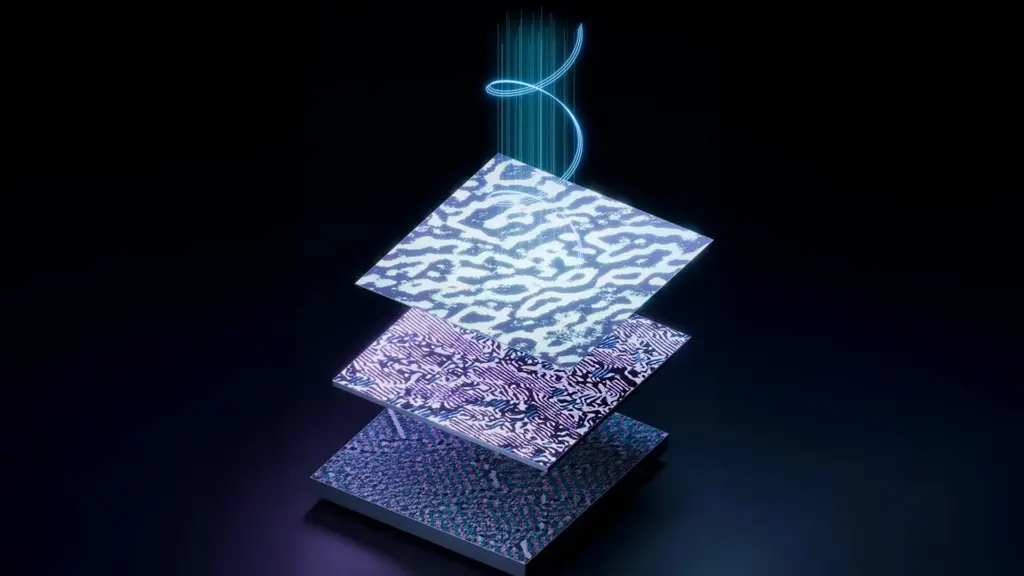
To solve this stubborn problem, the Brown University engineering team devised an entirely new method for producing thin films of bismuth ferrite that shields the material from structural degradation.
Instead of growing the material on standard substrates, the researchers carefully deposited the bismuth ferrite onto a foundational base made of dysprosium scandate, a specialized compound derived from rare earth elements. This underlying structural material features a crystal lattice with slightly smaller dimensions than bismuth ferrite, creating a deliberate mismatch between their respective atomic arrangements.
That precise structural mismatch places the overlying bismuth ferrite under continuous, uniform compression. This mechanical stress helps preserve the delicate atomic structure required for the material’s electrical and magnetic properties to remain completely intact, even at microscopic scales.
Furthermore, the team incorporated a second metallic layer strategically designed to counteract unwanted internal electric fields. By preventing those stray fields from disrupting the material’s electrical polarization, this additional engineering layer directly addresses the second major cause of the dead layer effect.
Combined together, these two distinct innovations allow the bismuth ferrite film to retain its valuable multiferroics properties even when it is reduced in thickness to just a few angstroms. But as the researchers analyzed their creation further, they discovered something unexpected that pushed the research into entirely new territory.
An Unexpected Form of Magnetism
Rather than simply preserving the material’s original capabilities in a thin format, the newly engineered atomic environment actually improved its magnetic behavior in a radical way.
The engineered layers caused the bismuth ferrite to exhibit altermagnetism, an unusual and newly prominent form of magnetism that ingeniously combines the most useful characteristics of two more familiar magnetic states: ferromagnetism and antiferromagnetism. This unexpected discovery could prove particularly important for developing faster, more compact computer components that do not suffer from the traditional trade-offs of magnetic data storage.
"Ferromagnets are useful for memory and logic because they produce strong magnetic signals that are easy to read out," Caretta explained. "The challenge is that they are relatively slow, and their stray magnetic fields make it difficult to pack devices densely on a chip without interference. Antiferromagnets can operate much faster and avoid those stray fields, but their signals are much harder to detect. Altermagnets are kind of the best of both worlds—they can be fast, densely integrated and still provide a strong electrical signal for readout."
In practical terms, altermagnets offer a valuable combination of operational speed, physical compactness, and easily readable electrical signals. These combined characteristics could help microelectronics engineers build advanced computer components that operate with extreme energy efficiency while avoiding the severe magnetic interference problems that plague conventional magnetic materials in high-density chip designs.
The remarkable ability to induce this specific, advantageous magnetic behavior within an exceptionally thin multiferroic film makes the discovery exceptionally promising for future semiconductor architectures.
A New Path Toward Energy-Efficient AI Computing
As the explosive growth of artificial intelligence continues to drive an unprecedented global demand for computational power, developing hardware that consumes significantly less electricity has become an increasingly urgent goal for both industry and environmental sustainability.
Caretta believes these fresh findings could help bring multiferroic materials significantly closer to practical, real-world use in low-power memory and advanced computing devices. Although the technology will still require further development, testing, and industry collaboration before it can be successfully incorporated into commercial silicon chips, the research successfully demonstrates that a long-standing materials science limitation can indeed be overcome.
Moreover, the project illustrates that carefully and creatively engineering a material’s atomic environment can achieve much more than merely preserving its existing bulk properties. Under the right experimental conditions, intelligent design can actually unlock entirely new, highly useful behaviors that were not inherently present in the original, natural material.
"We know the underlying properties are already there in the bulk materials," Caretta noted, reflecting on the broader implications of the work. "The trick is learning how to engineer them into a form that’s useful—and sometimes even better than what nature gives us."
The research team’s breakthrough was made possible with financial support from key federal funding agencies, including the U.S. Army Research Office under award number W911NF-21-2-0162, the National Science Foundation through grants DMR-2039380 and OIA-2327352, and the U.S. Department of Energy under contract DE-AC02-05CH11231.